A $400 Million Machine Is Deciding the Future of AI Chips
Nvidia has AMD. TSMC has Samsung and Intel. But when any of these rivals need to shrink transistors further, they all end up at the same company's door. That is why ASML's grip on the bottom layer of the AI chip stack keeps getting tighter.
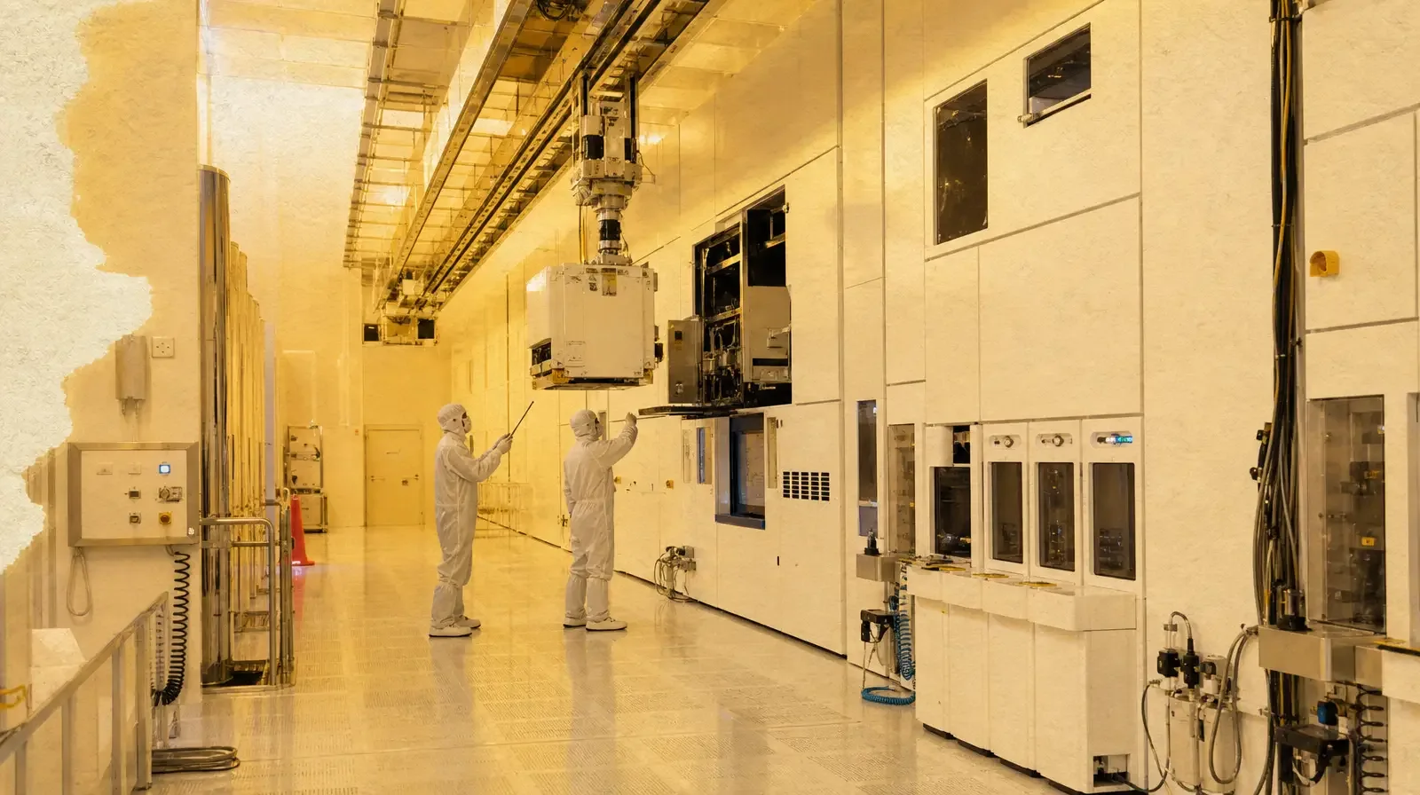
A $400 million machine is landing in chip fabs
One piece of semiconductor equipment. $400 million. The number alone is hard to square. That is roughly what it costs to build an entire factory in most manufacturing industries, spent instead on a single machine.
Yet customers are actually moving. According to Reuters, capacity on existing EUV machines is essentially booked out through 2027. Intel has moved fastest to adopt High-NA, the next-generation lithography tool. Samsung and SK Hynix plan to use it for DRAM production starting in 2028. TSMC expects to bring it in around 2030.
$400M — Price of a single High-NA EUV machine.
0.55 NA — Numerical aperture, up from 0.33 on existing EUV tools. Prints finer patterns in a single exposure.
94% — ASML's share of the entire lithography equipment market in 2025, as cited by Reuters.
High-NA does not need to be complicated
Think of a lithography machine as an ultra-precise camera that draws circuits onto a wafer. To draw smaller circuits sharply, you need shorter-wavelength light and better optics.
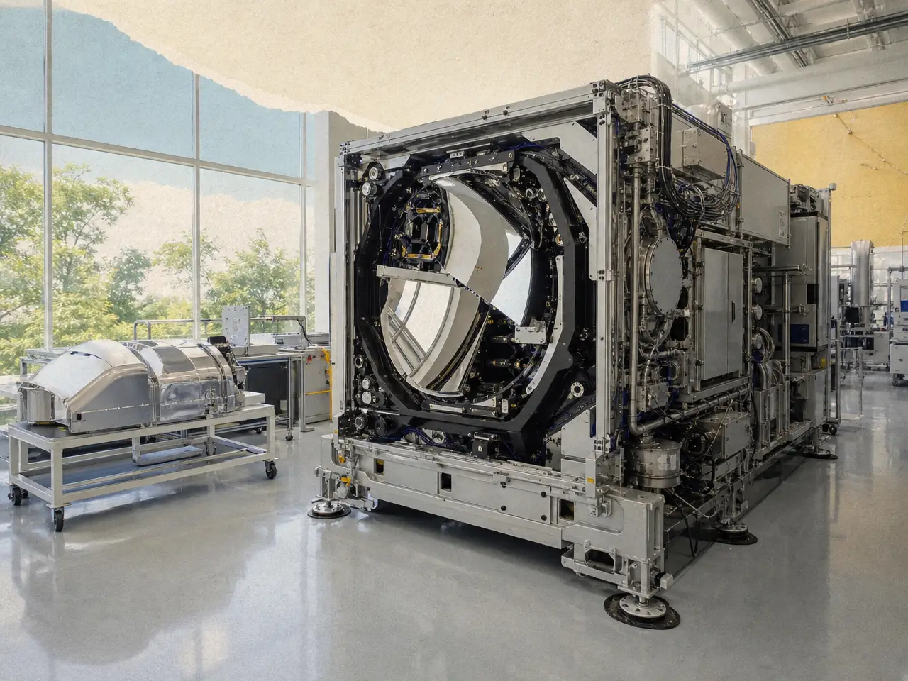
The "NA" in High-NA stands for Numerical Aperture, a measure of how widely and precisely a machine can gather light. Existing EUV tools run at 0.33 NA; High-NA runs at 0.55. ASML says this jump lets it print structures roughly 1.7 times smaller in a single exposure. In terms of area, that can translate into transistor density gains of up to 2.9 times.
But the real economics come from cutting process steps, not just shrinking line widths. ASML says that in some logic and DRAM processes, a single High-NA exposure can replace three to four exposures that would otherwise require multi-patterning on existing Low-NA EUV tools. On certain critical layers, the company has seen total process steps drop to roughly a tenth of what they used to be.
Multiple exposures do not just eat up more machine time. Each pass drags along coating, developing, etching and realignment steps. More steps mean more production time, more floor space and more chances for defects. If High-NA can deliver enough yield and throughput, the sticker price alone stops being a reliable guide to whether it pays off.
Go down the AI chip stack and the competitors disappear
The top of the AI industry is fiercely contested. Models compete among OpenAI, Google, Anthropic and xAI. Accelerators span not just Nvidia and AMD but custom silicon like Google's TPU and Amazon's Trainium. HBM memory is a three-way fight among SK Hynix, Samsung and Micron. Advanced foundry work splits between TSMC, Samsung and Intel.
- AI services and models — many competitors
- GPUs and custom ASICs — Nvidia, AMD, Google, Amazon and others
- HBM — SK Hynix, Samsung, Micron
- Foundry — TSMC, Samsung, Intel
- Advanced EUV lithography — effectively ASML alone
According to Reuters, ASML held about 94% of the entire lithography equipment market in 2025, and it has no meaningful commercial rival in EUV. Nikon and Canon operate in other lithography segments, but neither offers a viable alternative for mass-producing at the leading edge today.
This is where ASML's business becomes something sharper than the classic "picks and shovels" trade. When more companies chase gold, the shovel seller benefits. When more companies compete to build AI accelerators, more of them need leading-edge lithography. Regardless of who wins the GPU war, as long as the industry keeps shrinking transistors, ASML can sell to multiple winners at the same time.
Why shrinking transistors matters even more in the AI era
AI data centers are not a market that judges chips on raw performance alone. What determines server economics is how many tokens and how much computation you can process per unit of power. If a chip gets faster but also draws more power, a data center's power draw, cooling load and rack count all rise to match.
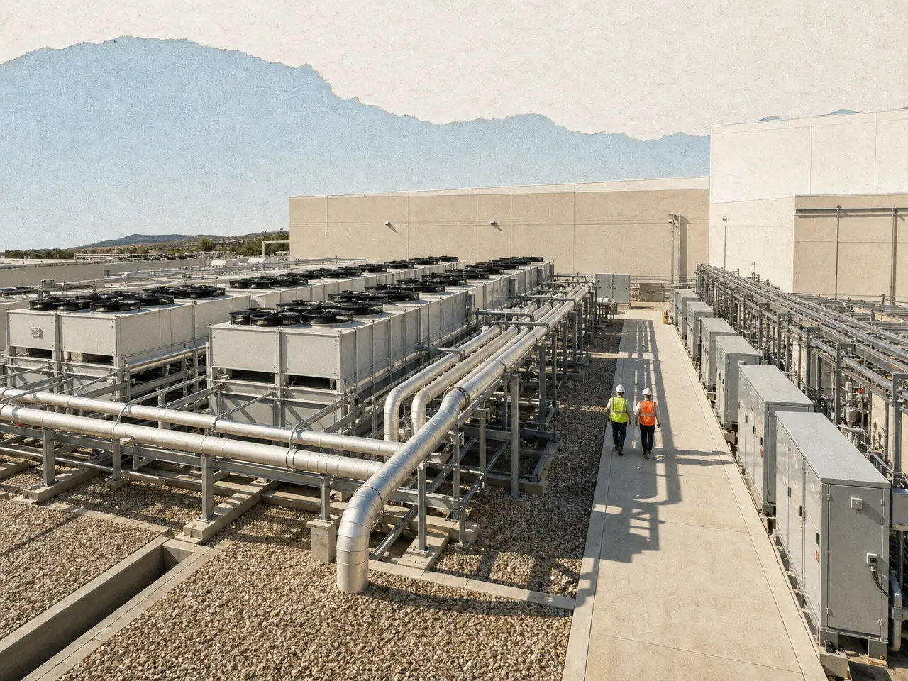
That is why performance per watt matters so much for AI chips. Making transistors smaller and packing more of them into the same area gives chipmakers room to improve performance and power efficiency at the same time.
The interesting paradox is that ASML does not benefit when Moore's Law gets easier. It benefits when shrinking transistors gets harder. Squeezing out the last few percentage points of performance and power efficiency requires more expensive equipment and more complex processes. Rising technical difficulty is precisely what turns into ASML's moat.
But High-NA is not printing every AI chip yet
There is an important counterpoint here. Today's High-NA tools can expose a smaller area in a single pass than existing EUV machines. That constraint bites hardest on the enormous data-center chips that Nvidia and Google use, since those dies are large.
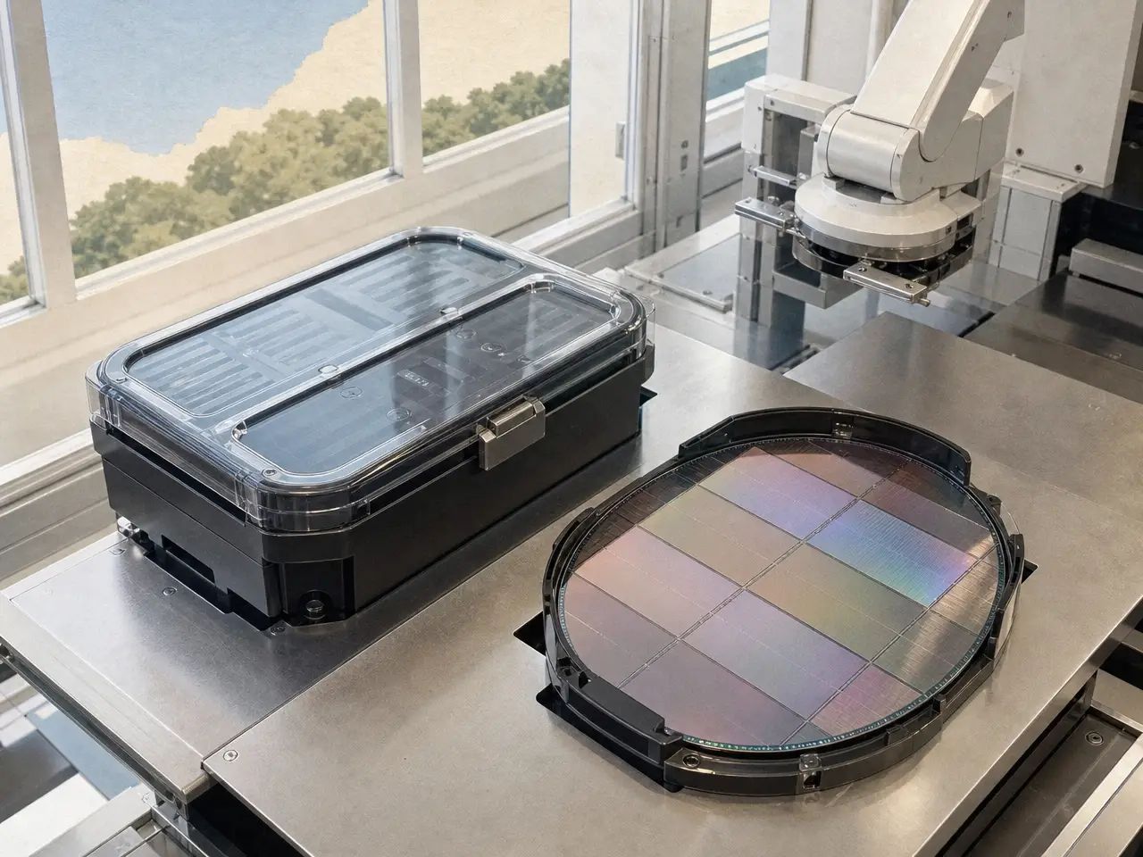
ASML is working with the industry to develop a larger mask format to solve this. The company is targeting a pilot line in 2031 and mass production in 2033. So the claim that "High-NA is already making every Nvidia GPU" gets ahead of where things actually stand.
The $400 million price tag is also a real burden for customers. If a layer is already economical using multi-patterning on existing Low-NA EUV tools, there is no reason to switch to High-NA. In the end, adoption speed will not be decided by the machine's price tag. It will be decided by yield, throughput and how many process steps each layer can cut.
Insight Times Editorial Desk