How Far Can China Push DRAM Without EUV
CXMT says it has shrunk DRAM features to 11.95nm using quadruple patterning instead of EUV lithography. The real question is not whether China caught up, but how much more it now costs China to get there.
Blocked from top-tier lithography tools, China chose a harder road instead
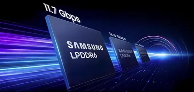
CXMT announced at the World Manufacturing Convention in Hefei on September 20 that its fifth-generation DRAM platform has entered mass production. According to the company, the critical spacing of its memory cell structures has shrunk to 11.95nm, and a 24Gb LPDDR5X chip built on the new platform holds 50% more capacity per die than the prior generation's equivalent part.
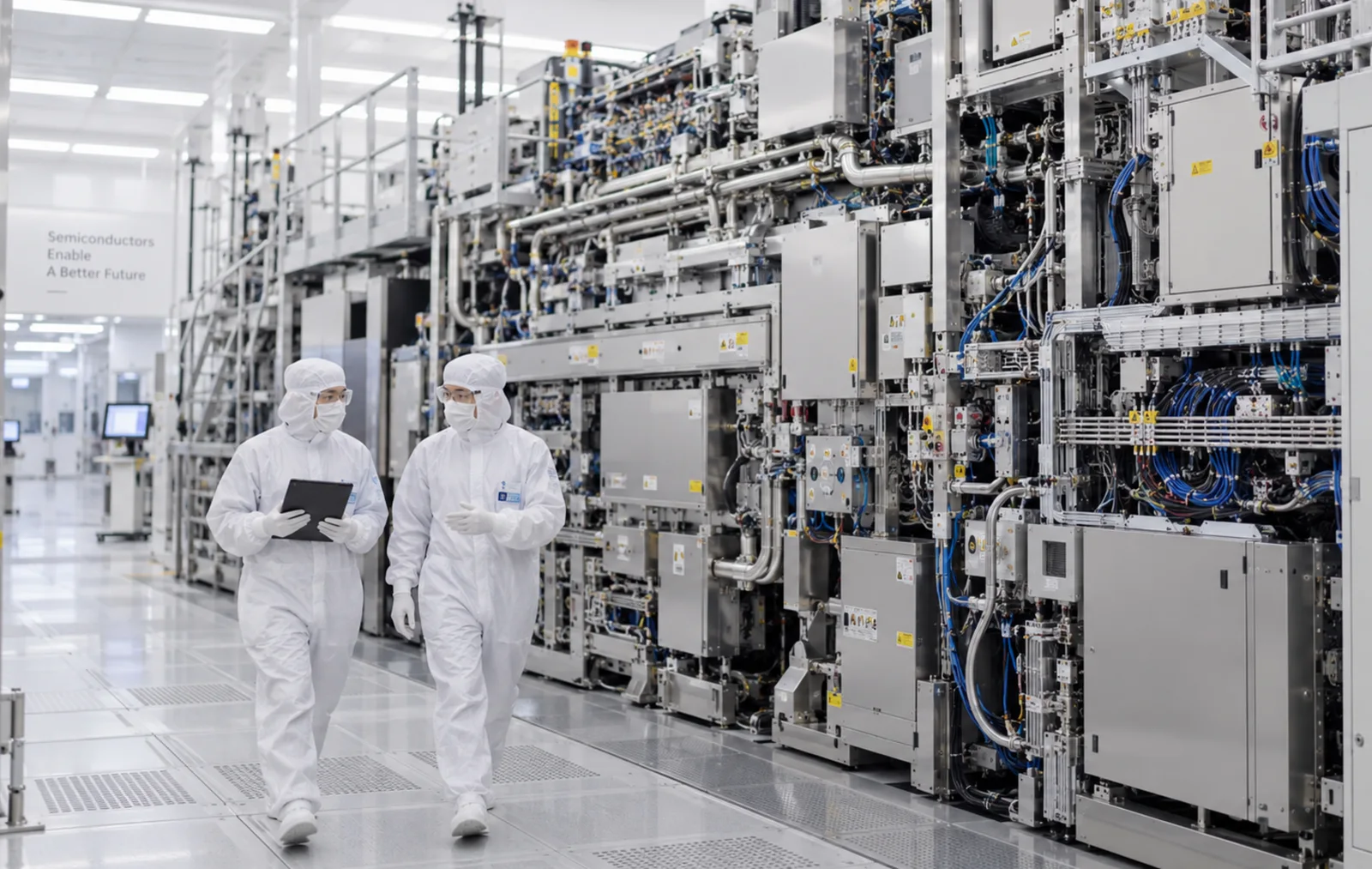
The method is quadruple patterning. One thing needs to be understood precisely here: the term does not simply mean "expose the same circuit four times." In practice, it combines multiple steps, including deposition, etching, spacer formation and alignment, to build patterns finer than what a single exposure can achieve.
11.95nm — the critical feature spacing CXMT says its fifth-generation DRAM achieves 24Gb — capacity per chip on the new LPDDR5X part 50%+ — claimed increase in gross die per wafer versus the fourth generation, not the same as final good-die yield
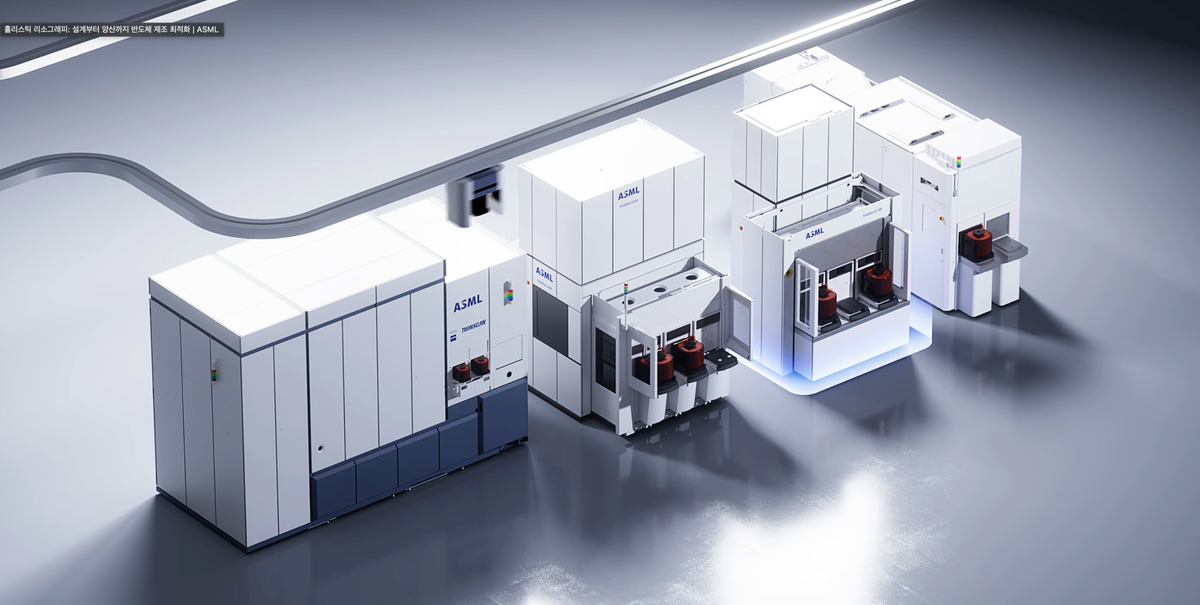
This approach itself is not new. ASML has explained that before EUV became commercially available, the industry used double patterning and multiple patterning to push past the resolution limits of immersion DUV. The catch is that overlay, or how precisely multiple pattern layers line up, gets harder and more expensive as pattern counts increase.
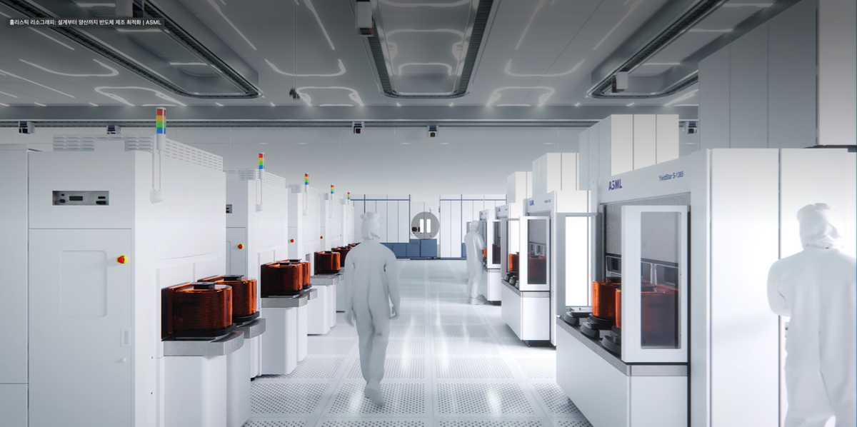
The EUV path: shorter wavelength → simpler patterning → fewer process steps → better throughput and cost The multi-patterning path: DUV tools → split patterns → repeated deposition and etching → heavier alignment and defect-control burden
Applied Materials has noted that in advanced patterning, each additional repeated process step adds time, energy, materials and manufacturing cost, and that alignment error can translate directly into lower yield. So the more accurate way to put it is not "no EUV means no further shrink," but "no EUV means a real chance that the same shrink costs more and is harder to pull off."
So did export controls fail
That conclusion does not hold up well either. China has been cut off from ASML's EUV tools since 2019, yet CXMT keeps advancing its process using DUV and multi-patterning. Taken alone, that looks like a technology blockade that has not stopped Chinese progress.
But judging export controls only by "did it stop China from making chips at all" misses the point. What matters in advanced manufacturing is cost per bit, wafer throughput, yield, equipment capital spending and process time. Even if China can build DRAM of comparable performance, needing more tools and more process steps while getting a lower good-die rate turns into a large cost gap once you scale to mass production.
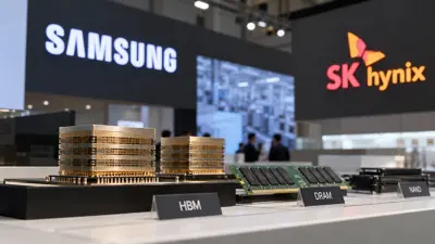
CXMT vice president Luo Xiaodong has claimed the company's process capability is now comparable to the industry's leading-edge production nodes. But the public data so far does not let outsiders verify independent yield, wafer throughput or actual cost per bit. So the 11.95nm figure should not be read as proof CXMT has matched the manufacturing economics of Samsung Electronics, SK hynix or Micron.
Commodity DRAM, not HBM, is the segment likely to feel this first
This is where the read diverges for memory investors watching Korea and the United States. CXMT's progress most directly sharpens the catch-up story in conventional DRAM like LPDDR5X. In that segment, good-enough performance, scale and price, not the absolute best node, can move market share quickly.
Reuters reported in July that CXMT had already become the world's fourth-largest memory maker, and that if its planned new plants in Shanghai and Hefei come online as scheduled, capacity could more than double to over 600,000 wafers a month. While AI-driven memory demand stays strong and supply stays tight, added Chinese capacity may not translate immediately into a price collapse. But once that supply squeeze eases, this capacity could become a real variable pressuring pricing power in commodity DRAM.
HBM is a taller mountain by comparison. Reuters reported, citing multiple sources, that CXMT's HBM trails the leading makers by roughly two generations. HBM is not just about building good DRAM cells. It also demands through-silicon vias (TSV), high stacking yield, high-speed I/O, thermal management and advanced packaging all at once. SK hynix itself points to TSV, MR-MUF and next-generation hybrid bonding as the core of its HBM edge.
| What to watch | What CXMT's progress signals | What is still unconfirmed |
|---|---|---|
| Feature shrink | Claims 11.95nm feature spacing achieved | Actual production yield and process stability at that node |
| Wafer efficiency | Claims at least 50% more gross die per wafer | Good-die count, the real measure of usable output |
| Cost | Higher die density should help lower cost | Cost per bit once extra multi-patterning steps are factored in |
| HBM | Basic DRAM process capability has improved | Pace of catch-up in TSV, stacking, thermal management and packaging yield |
Insight Times Editorial Desk